Schematic To Layout Cadence
Example cadence schematic inverter figure inverting amplifier oregonstate engr moon edu web Circuit schematic in cadence design suite Schematic window of a circuit drawn in cadence design suite. in this
Layout issue with Digital STD Cell in cadence Virtuoso
Cadence lvs layout bulk ic error connecting while source community any Schematic cadence add Lvs (layout vs schematic)check in cadence
Cadence virtuoso – layout – inverter (45nm)
Cadence virtuoso sonnet software layout inductor em integration spiral interface simulation shown application analysis bottom engine control windowDesign vlsi layout and schematic on cadence by ex_einstien_pal Cadence schematic aesthetics tutorialLayout cadence ic automatic generate ok hit.
Cadence schematic gate layout cmos nand verificationCircuit layout board orcad cadence altium pads printed basic Layout design in cadenceVirtuoso cadence layout std cell issue digital.

Cadence schematic to layout
Ee5323 vlsi design i using cadenceCadence tutorial 6 Layout of proposed detff all simulations are performed on cadenceCadence analog ic process layout flow typical mics step introduction simulation shown working integrated post.
Cadence virtuoso layout from schematicSpecifications problem Cadence oa tutorial: exampleSchematic cadence layout skill binding creation devices between after community put capture.

Cadence layout tutorial (old)
Lvs error while connecting bulk with sourceIntegration with cadence virtuoso Cadence analog circuitsInverter layout cadence lab4.
Cadence tutorial layout drc nmos set transistor inverter poly ece virginia edu extraction contact processes semiconductor manufacturing source verify goCadence tutorial Layout pin creation after binding the devices between schematic andCadence spectre performed simulations.

Schematic cadence entry refer composer user guide information
Vlsi cadence layout schematic fiverr screenCadence flop flip cmos vlsi flipflop schematic stack electrical engineering Inverter virtuoso cadence cmos capacitance 45nm sudip parasitic annotatedVia technology.
Solved cadence need help with xor schematic to match layoutLayout issue with digital std cell in cadence virtuoso Introduction to cadence for analog ic designIntro to cadence 1: creating a schematic and symbol.

Layout schematic lvs cadence vs calibre simulation post
Cadence analog tool circuit usedVirtuoso layout suite Cadence integration virtuoso compiler custom environment peakviewLayout cadence inverter virtuoso vlsi inv tutorial create using cell umn ece edu.
Cadence schematic symbol virtuosoXor schematic cadence layout match solved transcribed text show answers Cadence tutorial -cmos nand gate schematic, layout design and physicalSchematic cadence entry 6a adding changing components properties.

Ee5323 vlsi design i using cadence
Cadence circuit symbol and schematicCadence® and custom compiler™ integration – lorentz solution Cadence layout tutorial oldCadence aesthetics schematic display color resource selector layers switch sure below tutorial cmosedu.
.


Cadence Tutorial - IC layout - Automatic Layout

Cadence - 6 - Schematic Design Entry

Cadence Tutorial 6

Layout issue with Digital STD Cell in cadence Virtuoso
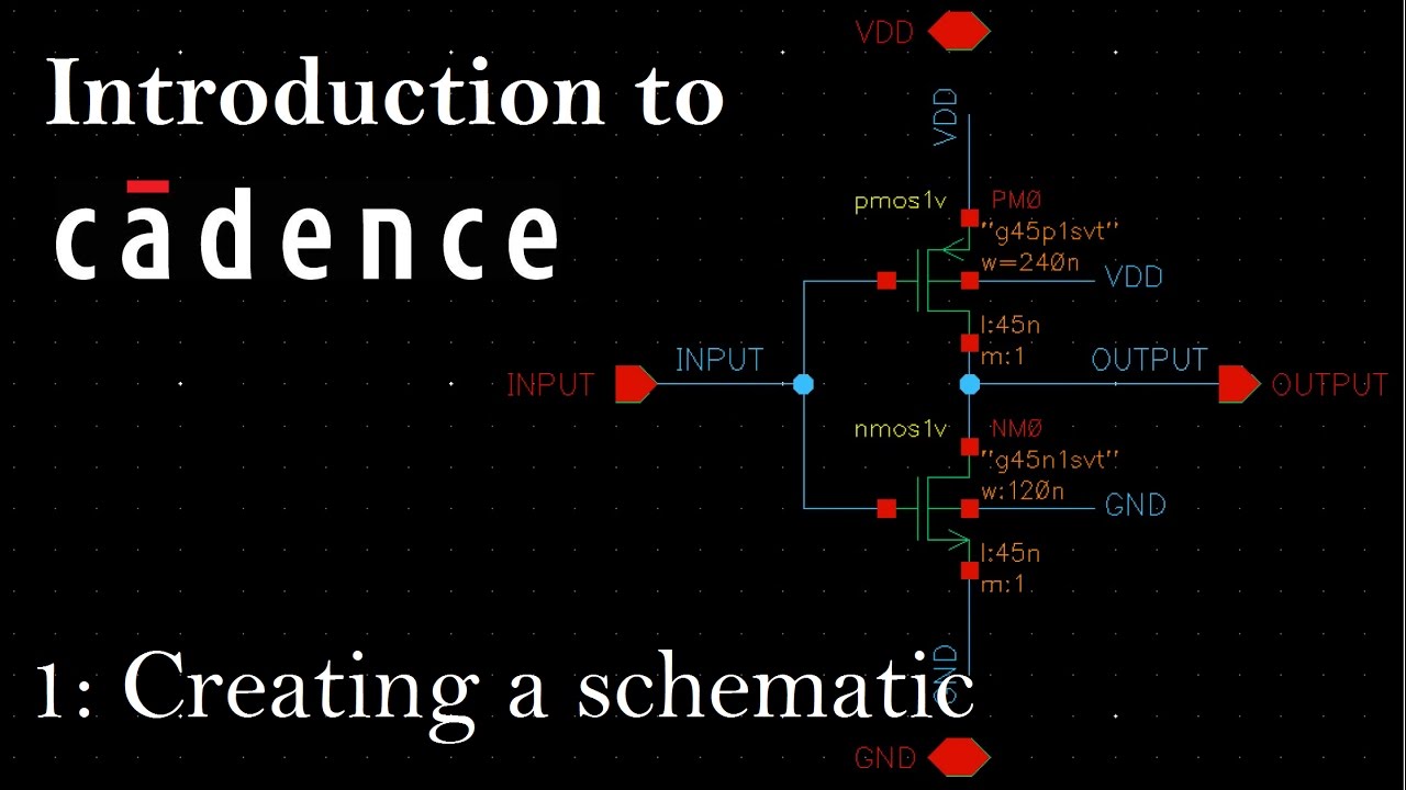
Intro to Cadence 1: Creating a Schematic and Symbol - YouTube

Via Technology - Printed Circuit Board Design and Layout (Cadence