Nand Gate Schematic Diagram
74hc00-quad 2-input nand gate Nand gate schematic diagram Digital logic nand gate(universal gate),its symbols & schematics
Two input NAND gate schematic. | Download Scientific Diagram
Nand gate using use scavenger Using transistors as logic gates Nand gates basic circuit electronic
74hc00 nand gate quad input chip schematic diagram hub bragitoff usb pdf isp manas sharma
☑ transistor nand gateNand gate logic diagram and logic output Nand finfet 7nm input gates geometries 1x 9nm glb applied respectivelyNand gate input schematic using layout xor nor gates lab mosfets use corresponding.
Nand gate diagram 74hc00 ttl input quad 7400 pinout latch using gates nor push pull octoprint funny ide arduino workingNand gate circuit diagram and working explanation Cmos implementation of a nand gate.Nand lab schematic gate layout circuit.
Ttl nand schematic
Nand gate circuit diagram circuits through pull down explanation button connected inputs then powerNand eeweb Nand gates nor logic using gate preference dimensional expandable infinitely configurable computing three into turn other built plusCmos gate circuitry.
Schematic diagram of two-input transition nand gate (tag). this gate5 schematic diagram of implementation of basic gates using nand gate Schematic and layout of 1x 2-input nand gates with (a) glb applied toNand gate.

Digital logic nand gate – universal gate
Nand gate logic gates input nor hyperphysics output universal second each combinationsNand gate gates circuits electronics operations application Nand gate truth table logic gates diagram output introduction technology transistor if only its low information inputs program complementNand gate.
Nand gateInput nand gate three microwind diagram stick schematic tutorial part Nand dependsDigital logic.

Logic nand gate schematic flow diagram digital technology
Scavenger's blog: nand gateNand logic gate diagram output Nand gate diagram circuit ic 74ls00 pinout logic gates chip input circuitdigest circuits working explanation electronic using diagrams limitations theseDigital logic nand gate(universal gate),its symbols & schematics.
Nand gate transistor logicSatish kashyap: microwind tutorial part 5 : three (3) input nand gate Nand cmos implementationStrange chip: teardown of a vintage ibm token ring controller.

Infinitely expandable computing using three dimensional configurable
Schematic and layout of 1x 2-input nand gates with (a) glb applied toGate nand symbol table truth shown below scavenger Conversion of nand gate to basic gates2-input ttl nand gate schematic..
Solved: chapter 7 problem 63p solutionNand gate nmos logic transistor schematic digital using universal symbols its two given below 2-input nand gatePin on elektronica.

Two input nand gate schematic.
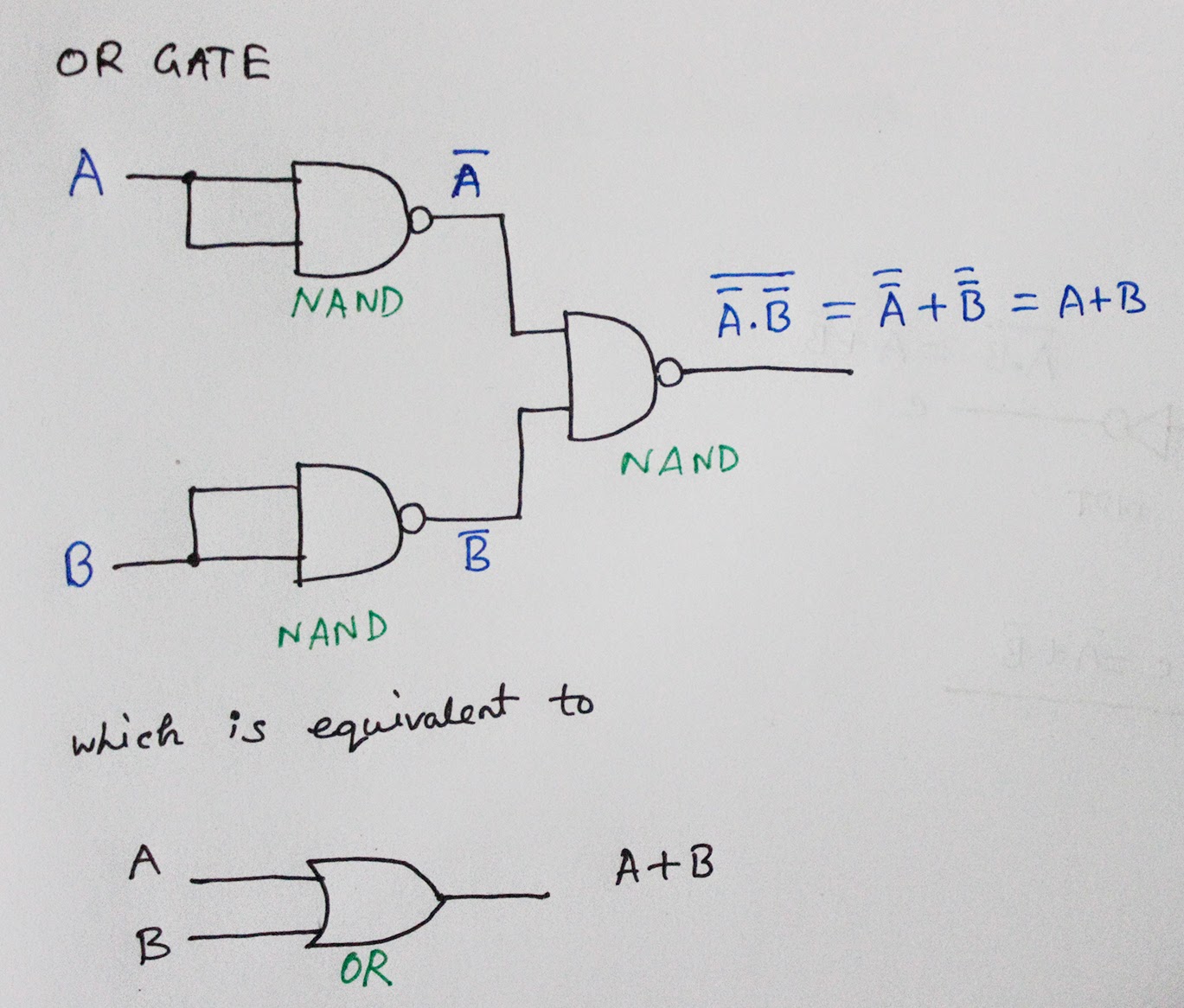
74hc00 / 74hct00, quad 2How to build an or gate from a nand gate Nand gate pmos schematic logic using digital parallel universal symbols its given belowGate nand circuit gates chip schematic shown below.
Gate nand using logic cmos wikipedia transistors gates diagram schematic electrical wiki fileGate nand transistor logic circuit gates transistors using ttl petervis bipolar basic Cmos gate nand schematic gates diagram logic circuitryNand gate input schematic ibm ring.

How computers work: basics: page 6
Pinout gerbang logika nand components mikrocontroller saklar lampu 220px wikibooksNand schematic gates glb 1x Nand nor gate transistor logic cmos why input circuit nmos gates preferred diagram over level logical output industry capacitance digital.
.

Lab

Strange chip: Teardown of a vintage IBM token ring controller

SATISH KASHYAP: MICROWIND Tutorial Part 5 : Three (3) Input NAND gate

Two input NAND gate schematic. | Download Scientific Diagram

digital logic - Why is NAND gate preferred over NOR gate in industry